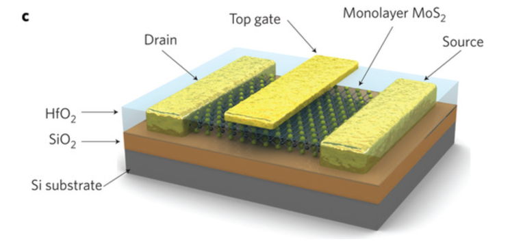
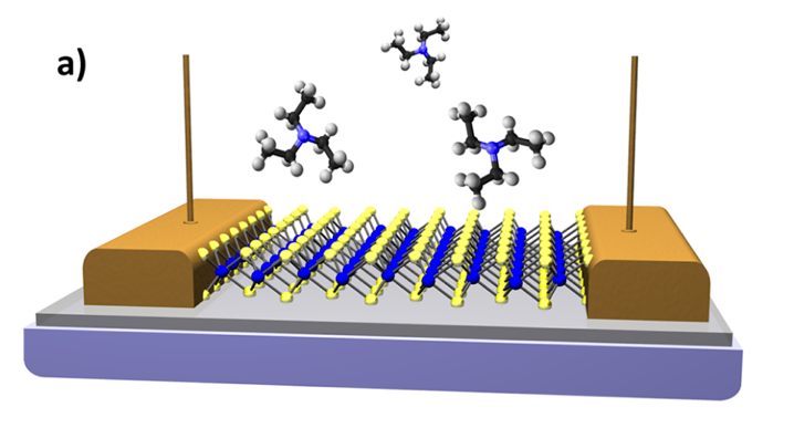
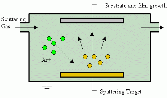
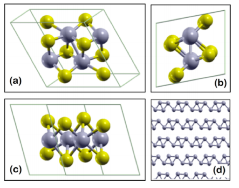
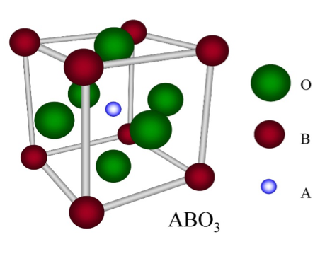
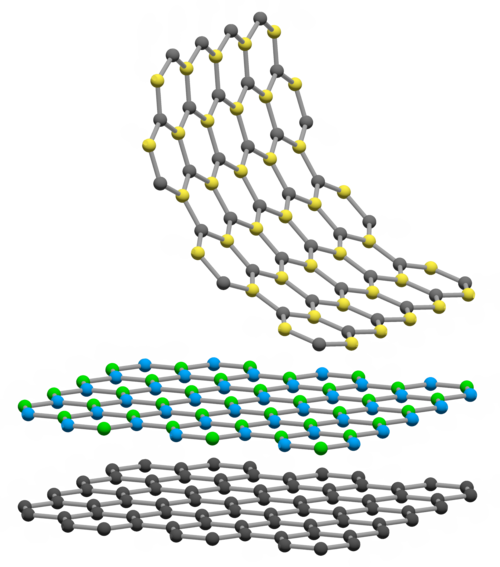
2D Materials and Thin Films

Condensed Matter Physics - Centre for Doctoral Training

CDT_Background Created with Sketch. Natasa Vasiljevic Kei Takashina Simon Bending Martin Gradhand Daniel Wolverson Chris Bell Marcin Mucha- Kruczynski Synthesis of Thin Films Why use Thin Films? What are 2D Thin Films? Examples of TMDs TMD and Graphene Synthesis History of TMDs Why Use TMDs? Transition metal dichalcogenides! TMDs How did we find Graphene? Graphene - What is it?! What is 2D? Click here to see the Academics!
cross Created with Sketch.

WHAT IS 2D?


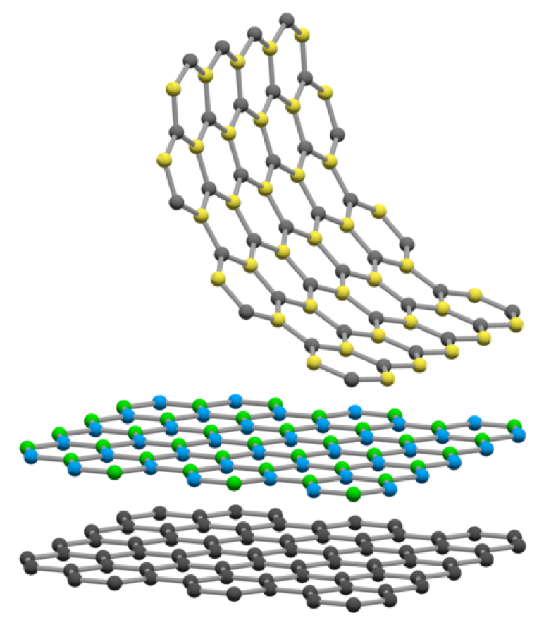
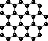
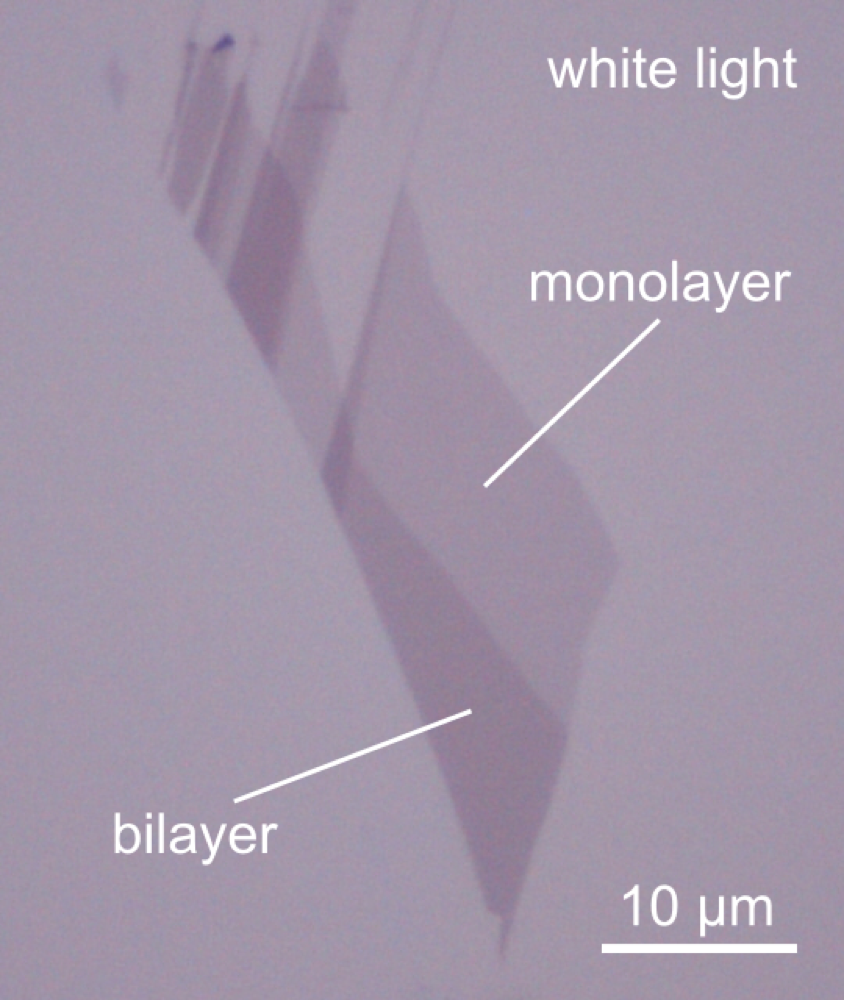
Determining which materials can be considered as two-dimensional is not clearly defined. A strict definition could limit this class of materials to the crystalline materials consisting of only a single layer of atoms. This would limit the discussion to graphene-like materials and transition metal dichalcogenides (TMDs). In photonics however, 2D materials are all materials whose thicknesses are considerably smaller than the wavelength of the light used. Another definition could be any material where the physics is constricted in one of the spatial dimensions, since the properties of thin films can differ from their bulk equivalents. For superconducting materials, the thickness becomes relevant if it is smaller than the materials’ penetration depth. In order to keep the subject broad, we have decided to include any materials where the reduced dimensionality influences the material’s properties. This includes materials with interesting surface or interface physics, few-layered materials and thin films.

cross Created with Sketch.

WHAT IS GRAPHENE?


Graphene consists of a single layer of carbon atoms arranged in a hexagonal honeycomb-like structure. The bonds between the carbon atoms within this layer are extremely strong, making graphene the strongest material in the world. Remarkably, it also has high elasticity, as it can stretch up to 25% without breaking. But graphene is not only extremely strong, light and thin. It also has very high heat and electrical conductivity.

The two dimensional (2D) hexagonal carbon lattice offers very little resistance for electrons. In fact, the electrons in graphene move like massless relativistic particles, which we call Dirac electrons, moving at a constant speed that is about 300 times smaller than the speed of light, making graphene a possible playground for studying quantum electrodynamics (QED). One of the peculiar properties of Dirac electrons is the ability to tunnel through a barrier with a probability of 100%, called Klein tunnelling, which would be impossible for classical electrons.

Since graphene is atomically thin, it is also highly transparent. This, in combination with high strength and conductivity makes it an interesting candidate for transparent and flexible touch screens, low-loss nanoscale electronic devices, solar cells and more. Graphene can also be seen as a very thin atomic mesh, which has very high impermeability and could be used as gas sensors or membranes for e.g. hydrogen fuel cells.

ARPES image of graphene.

cross Created with Sketch.

THE HISTORY OF GRAPHENE


Graphene, the atomic layer that makes up graphite, was first studied in 1946, when a paper by P.R. Wallace studied its electronic properties and noted the unusual behaviour of the Dirac electrons. At the time, two dimensional materials were thought to be thermally unstable, as predicted by Peierls and Landau and the results were merely used as a first step to describing the electronic properties of graphite.

It was not until the isolation of a single layer of graphene in 2004 by A. Geim and K. Novoselov in Manchester that research towards graphene really took off. The researchers managed to isolate graphene using mechanical exfoliation, where they basically use some sort of scotch tape to split a graphite crystal into as few layers as possible. The critical part of their project was the observation that graphene became visible under a microscope when placed on a silicon wafer with a carefully chosen thickness of silicon oxide.

Their groundbreaking experiments regarding graphene earned the two researchers a Nobel prize in 2010. In the decade after the isolation of graphene, thousands of papers got published on graphene and related materials, and the original paper by Geim et al. is now one of the top 100 research papers of all time.

cross Created with Sketch.

WHAT ARE TRANSITION METAL DICHALCOGENIDES?


Transition metal dichalcogenides (TMDs) are layered structures (like graphite) which have strong covalent bonding in plane and weak van der Waals’ forces separating the layers when in the bulk form. TMDs have the form MX2, where M is a transition metal like Mo (Molybdenum) or W (Tungsten) and X is a chalcogen like S (Sulphur) or Se (Selenium). TMDs, like graphite, can be separated into single layers, and these monolayer forms have very interesting properties.

A MoSe2 monolayer.

The monolayer structures are 2D, like graphene, however have proved to be perhaps more interesting than graphene, due to the band gaps present in most, which make them semiconductors and thus useful in devices such as transistors. TMDs in the bulk form can exist as one of three different polymorphs: 1T (trigonal), 2H (hexagonal) and 3R (rhombohedral). The electrical properties of approximately 40 known layered TMDs range from metallic and half-metallic to semiconducting, and some materials exhibit superconducting and charge density wave behaviour.

The structure of ReSe2.

When monolayers are separated, these properties may change: for example, MoS2 is an indirect band-gap semiconductor when in bulk form, but becomes a direct bandgap semiconductor in the 2D form. This makes monolayer MoS2 extremely useful in areas such as optoelectronics, because photon absorption can cause electrons to jump from a valence state to a conducting state without the need for interaction with phonons.

cross Created with Sketch.

WHY USE TMDs?


TMD monolayers such as MoS2 and WS2 have applications in digital electronic devices due to their direct band gaps. In electronics, transistors operate logic gates which require a distinct “on” and “off” state. If the band gap is too small, the transistor may accidentally switch between the two states (for example, due to an increase in temperature). MoS2 and WS2 monolayers have large band gaps, which lead to a large on/off ratio, making them reliable in transistors.

Field Effect Transistor (FET): Figure 2c from Radisavljevic, Branimir, et al. “Single-layer MoS2 transistors.” Nature nanotechnology 6.3 (2011) : 147-150.

Due to the presence of a direct band gap and reasonably high mobility, monolayer TMDs show potential to be used in solar cells. However, the efficiency is currently hindered due to limited absorption which depends on thickness. Research is being conducted to overcome this, and some possible solutions include using vertical stacks of monolayers and varying strain which could be used to trap more light.

Light-emitting diodes (LEDs) also use direct band-gap materials, and monolayer TMDs are being currently studied for use in LEDs. They have the advantage of being extremely thin and flexible. Current issues include difficulty in controlled doping and relatively low efficiencies compared to organic LEDs, however monolayer TMDs could become very competitive if improvements are made to doping methods and surface engineering.

TMD monolayers used in sensors: Figure 1a from Perkins, F. K.; Friedman, A. L.; Cobas, E.; Campbell, P. M.; Jernigan, G. G.; Jonker, B. T. Chemical Vapor Sensing with Monolayer MoS2. Nano Lett. 2013, 13, 668–673.

Another application of TMDs is in sensors. When an analyte binds to the surface of a sensor there is a change in the electronic properties. When the sensor consists of a bulk material, this change is very small and difficult to detect, since the binding occurs on the surface. However, in the case of monolayer TMDs, the surface area to volume ratio is high, which means that the change is significant and therefore can be detected, which makes it useful in sensors.

cross Created with Sketch.

A HISTORY OF TMDs


TMDs were studied since the early 1960s, and exfoliation methods like the “Scotch tape” method were used by researchers such as Abe Yoffe in the 1960s and 1970s. Abe Yoffe says in a letter to Daniel Wolverson, that his “supervisor Philip Bowden from Caius College came back to England from Japan with a big crystal of MoS2 in a tobacco box”, which he took and “using scotch tape obtained a thin enough sample from it”. Therefore, a lot of interest was present in TMDs and even “thin layers of graphite”, which may have been monolayers of graphite (graphene). However, the main problem was that these monolayers could not be characterised, and techniques such as AFM (Atomic Force Microscopy) or Raman spectroscopy are now used to confirm monolayers. Therefore, the characterisation of graphene lead to a re-kindling of interest in TMDs and TMD monolayers.

Dr. Abe D. Yoffe

cross Created with Sketch.

SYNTHESIS OF GRAPHENE AND TMDs


In order to separate monolayers from the bulk, van der Waals’ forces between layers must be overcome.

Mechanical Exfoliation

Scotch tape can be used to get monolayers of graphite (graphene) or 2D-TMDs. The tape is stuck onto the bulk material and pulled off, and characterisation techniques such as Atomic Force Microscopy (AFM) may be used to check the number of layers (one or more) which were exfoliated. This technique is easy to perform, but a disadvantage is that it is difficult to control the number of layers formed.

Mechanical exfoliation using the “Scotch tape” method: Figure 1 from Novoselov, K. S., and AH Castro Neto. “Two-dimensional crystals-based heterostructures: materials with tailored properties.” Physica Scripta 2012.T146 (2012): 014006.


Chemical Exfoliation

There are various chemical exfoliation methods which are used to obtain 2D materials. Two common methods include ion intercalation and sonication in solvents. In ion intercalation, ions intercalate between layers of the crystal, expanding the crystal and weakening the van der Waals’ forces. Thereafter, methods such as ultrasonication or thermal agitation are used to obtain monolayers. Another method is the use of sonication, in which sound energy is used to separate layers, which are put in a suitable solvent, preventing the monolayers from re-aggregating.

Chemical exfoliation of MoS2 using ion intercalation: Figure 1b from Zheng, Jian, et al. "High yield exfoliation of two-dimensional chalcogenides using sodium naphthalenide." Nature communications 5 (2014).

Chemical vapour deposition (CVD)

Chemical vapour deposition (CVD) is a common method used for synthesizing 2D materials. With reference to monolayer TMDs, it involves coating a substrate material such as silicon with a thin layer of the transition metal using physical vapour deposition (PVD) and subsequently exposing it to a chalcogen atmosphere. Controlling the thickness of the coating makes it possible to control the number of layers of TMD formed. Large areas of single-layer TMDs have been grown using this technique. To synthesize graphene, the CVD technique uses, for example, copper or nickel foils, on which graphene is grown using a mixture of methane and hydrogen and temperatures of about 1000°C.

Wet Chemical Methods

Nanosheets are formed in solution using wet chemical techniques. Appropriate transition metal and chalcogen reagents react to form TMDs, which intrinsically form nanosheets due to their layered nature. Graphene is commonly formed by the chemical reduction of graphite oxide. These methods are highly useful, but have some disadvantages such as problems with purity and yield, in addition to the difficulty of restricting vertical growth while allowing lateral growth.

cross Created with Sketch.

SOME EXAMPLES OF TMDS


Some examples of TMDs are given below, classified according to their properties:

Metallic: VSe2
Semi-metallic: MoTe2
Semi-conducting: TiS2, MoSe2, WS2
Superconducting: NbSe2
Magnetic: CrSe2
Charge Density Wave: TaSe2

cross Created with Sketch.

WHAT ARE THIN FILMS?


Thin films are materials whose thickness can range from tenths of a nanometer to a few microns. Thin films usually consist of a few layers of a material which has been deposited onto a substrate surface. Thin film preparation methods include chemical vapour deposition (CVD), epitaxy and physical vapour deposition (PVD). Since the surface-area to volume ratio is high, the properties of thin films may vary from those of the bulk. For example, thin films of a particular material may be of a different colour to that of the same material in bulk. Furthermore, electronic properties such as conductivity may be enhanced.

Thin films are useful because of their small size, flexibility when printed on materials such as plastics, cheap costs and their enhanced properties due to their 2D-like nature. A few applications include optical coatings, solar cells and batteries.

cross Created with Sketch.

WHY USE THIN FILMS?


Thin films can be used as decorative, optical and protective coatings and they also have applications in solar cells and in batteries.

Coatings

Thin films can be used as decorative coatings. For example, thin film coatings can be used on other surfaces such as glass to give it a certain colour. For example, a 0.09 micron thick layer of PbS (lead sulphide) thin films have been created to display a purple colour.

Thin films can be deposited on lenses or mirrors, which would modify the reflection and transmission properties of the lens or mirror. In this way, anti-reflective and high-reflectance surfaces have been produced.

Thin films can also be used to protect other surfaces, for example: Magnesium is prone to corrosion, and this can be prevented by applying a thin film coating of CrN (chromium nitride).

Solar Cells

Thin films of a photovoltaic material can be deposited on a surface such as glass or plastic. Using thin films means that the amount of active material in the cell is small, since the thin film is usually between two planes of glass. Thin films have the advantage of being cheaper than conventional solar cells, however the efficiency has been lower. Nevertheless, the efficiency is being continually improved, and thin film technology shows great promise for the future.

Some examples of thin film photovoltaics include Cadmium Telluride (CdTe), Copper Indium diselenide (CIS) and amorphous Silicon (a-Si).

Batteries

Thin film lithium batteries contain lithium polymers of a few microns thick deposited on various substrates, allowing the battery to be only a few millimeters thick. Thin film batteries are useful because of their small size, and can even be made flexible by printing onto plastic, metal foil, etc. A few applications of thin film batteries are: implantable medical devices, wireless sensors, phones and laptops.

cross Created with Sketch.

SYNTHESIS OF THIN FILMS


The synthesis of thin films requires depositing a layer of the material on a substrate, preferably with some control over the thickness. Deposition techniques are either chemical or physical in nature.

Chemical Deposition Techniques

For chemical deposition techniques, a fluid substance will have a chemical reaction with a surface, leaving a solid layer on top of the substrate. One example of this is plating, where a metal coating is deposited on a surface through a water solution with a salt of the metal. For chemical solution deposition a liquid precursor is used. This solution can be deposited on a flat substrate which is then spun at high velocities to centrifugally spread the solution over the substrate, a process known as spin coating. Thermal treatment then crystallizes the liquid film, leading to an even coating with controllable thickness. Another coating technique is dip coating, where a substrate is submerged in a solution and then withdrawn with care, where the thickness and homogeneity can be controlled by evaporation conditions, solution viscosity and withdrawal speed. For chemical vapour deposition, a gaseous precursor is used, but the principle is very similar. A specific type is atomic layer deposition, where the chemical process is divided into two steps. One reactant is deposited first, and another second, which guarantees total layer saturation, allowing the deposition of one atomic layer at a time.

Physical Deposition Techniques

For physical deposition techniques, the general process is to give the material to be deposited high energy, making highly energetic particles escape its surface. When these highly energetic particles come into contact with the cool surface of the substrate, they lose their energy and form a solid film on the surface. There are many ways of doing this, an electron gun can boil a material locally, a focused laser can vaporize a spot and convert the material into plasma. Magnetic sputtering relies on a plasma knocking a few atoms from a surface, which are then directed towards a surface using a magnetic field. In molecular beam epitaxy, a slow stream of atoms is directed at a surface, allowing epitiaxial growth one layer at a time. Once the particles hit the colder surface, their remaining energy will determine the quality of the resulting layer. When the substrate is too cold, the atoms will have no kinetic energy left to move around. This freedom to move around is useful, since the particles can find an energetically favourable position on the substrate, leading to better crystal quality and control over the layer thickness.

cross Created with Sketch.

Dr. NATASA VASILJEVIC

University of Bristol

Surface Physics Group

Electrochromic Properties of WO3

http://www.bristol.ac.uk/physics/people/natasa-vasiljevic/


Dr. Natasa Vasiljevic works in the surface physics group at the University of Bristol. Much of her work involves the electro-deposition of metals to control the growth of thin films. By changing the growth parameters of the thin films, properties such as optical and catalytic interactions can be changed. Recently Dr. Vasiljevic has been looking into the properties of electrochromic materials and is currently supervising a project on the analysis of WO3 thin films. WO3 changes from transparent to a translucent blue colour when an electric field is applied. A video of the effect is shown below.

The colour switching of WO3 works due to the incorporation of hydrogen ions into the perovskite structure when an electric field is applied. The effect is easily reversed by switching the electric field. Electrochromic materials could be used for many applications including smart windows, displays and mirrors.

An image showing the WO3 in a) its transparent state and b) its translucent state. Tungsten atoms are shown in blue, oxygen atoms in red and hydrogen in grey.

cross Created with Sketch.

Prof. SIMON BENDING

University of Bath

Centre for Nanoscience & Nanotechnology

Correlated Electron States in 2D Materials

http://www.bath.ac.uk/physics/contacts/academics/simon_bending/


Prof. Simon Bending works in the Centre for Nanoscience & Nanotechnology and the Department of Physics at the University of Bath. His research targets an understanding of the magnetic properties of superconducting and ferromagnetic materials at the nanoscale using Hall probe magnetic imaging and magnetotransport measurements. His current research focusses on the investigation of novel correlated electron states induced in molecular layers of 2D materials at very high carrier concentrations. Field effect ‘doping’ with ionic liquid gates is being used to induce very high charge densities in few-layer graphene and transition metal dichalcogenide (TMD) samples, allowing the evolution of insulating, metallic and superconducting states to be systematically followed. Other types of correlated electron phases such as ferromagnetism and charge density waves are also being sought or manipulated at extremely high carrier densities.

2H-TaS2 is a superconducting TMD which has a low bulk critical temperature of 0.8K. It has recently been shown that this is substantially enhanced in very thin few-molecular-layer flakes, reaching 2.2K in the thinnest (~3.5 nm) samples studied [1]. We have demonstrated that even larger enhancements of the critical temperature up to 4.7K can be induced in thicker 2H-TaS2 flakes using a DEME-TFSI ionic liquid top gate. Superconductivity is known to compete with charge density wave formation in 2H-TaS2 and one objective of our research is to obtain a detailed understanding of the evolution of these correlated electron states as a function of chemical potential, temperature and magnetic field.

[1] Navarro-Moratalla et al., Enhanced superconductivity in atomically thin TaS2, Nature communications 7, 11403 (2016).

cross Created with Sketch.

Dr. MARTIN GRADHAND

University of Bristol

Theory Group

Charge and Spin Transport in Metals and Superconductors

http://www.bristol.ac.uk/physics/people/martin-gradhand/


Dr. Martin Gradhand is interested in charge and spin transport in metals and superconductors, which he studies through first principles calculations. In the context of two-dimensional materials, Martin and his collaborators studied the impact of electron-impurity scattering on the spin relaxation time in graphene. Graphene has low spin-orbit coupling and is therefore expected to have long spin lifetime, which is of great interest for spintronics applications. Experimentally however, spin relaxation is consistently measured to be quite fast. The research assumed carbon and silicon adatoms as common impurities in graphene, and showed that these space inversion symmetry breaking adatoms acted as spatial spin hot spots, causing spin relaxation rates several orders of magnitude larger than symmetry conserving impurities, comparable to the experimental observations.

Together with scientists in Germany, he has also studied the spin Hall effect (SHE) in ultrathin noble-metal films with substitutional Bi impurities, where they predicted colossal spin Hall angles up to 80%. This enhancement of the SHE is caused by the reduced sample dimension and resonant impurity scattering. This resonant impurity scattering can be tuned by strain engineering. The giant SHE can be exploited to create materials with highly efficient charge to spin current conversion, another area of interest for spintronics applications.

cross Created with Sketch.

Dr. DANIEL WOLVERSON

University of Bath

Spectroscopy and Imaging Group

Spectroscopy of Transition Metal Dichalcogenides

http://www.bath.ac.uk/physics/contacts/academics/daniel_wolverson/


Dr. Daniel Wolverson is interested in the spectroscopy of semiconductors and uses techniques such as Raman microscopy to investigate the electronic structure of transition metal dichalcogenides (TMDs).

The Raman Spectrometer in the University of Bath.

An example of his current research involves the study of ReSe2 (rhenium diselenide) and ReS2 (rhenium disulphide) using Raman spectra and DFT (density functional theory) calculations. His research has shown that the number of layers and the orientation of ReSe2 or ReS2 flakes can be measured using Raman spectroscopy. Raman spectra have also been able to show the in-plane anisotropy in ReSe2. Dr. Wolverson has also explored magnetism in TMDs. His group is currently conducting experiments using ARPES (Angle-Resolved Photoemission Spectroscopy) in order to get a picture of the valence band structure for bulk and few-layer ReS2 and ReSe2, which can be compared to first-principles calculations using DFT.

Wolverson, Daniel, et al. "Raman spectra of monolayer, few-layer, and bulk ReSe2: an anisotropic layered semiconductor." Acs Nano 8.11 (2014): 11154-11164: Figure 1. Crystal structure of ReSe2; the rhombohedral unit cell of bulk ReSe2 (yellow, Se; gray, Re) oriented to the (a) ab, (b) bc, and (c) ca planes. (c) Different displacements of the Se atoms normal to the layer plane. (d) In-plane

cross Created with Sketch.

DR. MARCIN MUCHA-KRUCZYNSKI

University of Bath

Theoretical and Computational Physics

Theoretical Graphene Calculations

http://www.bath.ac.uk/physics/contacts/academics/marcin-mucha-kruczynski/


Dr. Marcin Mucha-Kruczynski is a theorist whose research interests include the study of the physical properties of two-dimensional crystals such as graphene and monolayer transition metal dichalcogenides (TMDs). He is interested in researching the optical properties of graphene and also studying the effect of strain on the electronic properties of graphene. Other interests include the study of graphene hetereostructures: for example, graphene placed on top of hexagonal boron nitride (hBN).

Bilayer graphene band structure: The whole Brillouin zone up to 3 eV from the neutrality point. Low-energy bands are shown in blue and split bands in yellow.

Graphene/h-BN moiré superlattice. The black dots denote the carbon atoms in graphene, while the red and green dots show the boron and nitrogen atoms in hBN. The yellow rhombus depicts the superlattice unit cell.

Watch Dr. Mucha-Kruczynski's Lecture on graphene

cross Created with Sketch.

DR. CHRIS BELL

University of Bristol

Correlated Electron Systems

Two Dimensional Electron Transport

http://www.bristol.ac.uk/physics/people/chris-bell/


Dr. Chris Bell is interested in the creation and control of novel electronic phases of matter in metals, semiconductors and insulators. His focus has recently been on low dimensional systems, which has included two-dimensional superconductors with low density and high mobility as well as ultrathin ferromagnets.

Perovskite structure with the chemical formula ABO3

An example of his research is ultrathin ceramics. Ceramics have interesting properties, for example: they can be semiconducting, insulating or metallic, can exhibit high temperature superconductivity, and be ferroelectric. Dr. Bell’s research focuses on combining individual ceramic crystal structures to form new materials. His research involves understanding the physics at the interfaces of these ceramic building blocks, and uses techniques such as low temperature magnetotransport to examine the emergent electronic properties of the new structures created.

Two perovskite structures combined to form a structure which now has the form AB0.5B’3O3 just at the interface

cross Created with Sketch.

DR. KEI TAKASHINA

University of Bath

Silicon Quantum Transport

Low-Dimensional Semiconductors

http://www.bath.ac.uk/physics/contacts/academics/kei_takashina/


Dr Kei Takashina is interested in the physics and applications of low-dimensional systems, particularly two dimensional electron and hole gases in semiconductor structures. At present his research focuses on silicon / silicon dioxide nanostructures for generating coupled low-dimensional systems. Using appropriate gate voltages, Dr Takashina and his associates are able to generate a two dimensional electron or hole gas (2DEG or 2DHG) near the silicon / silicon dioxide interface.


With the help of a magnetic field they can study spin and valley polarization in this system, as well as the coupling between electrons and holes when these are generated simultaneously in close proximity. Dr Takashina and his fellow researchers showed that valley polarization in silicon helps spin alignment at low electron densities, which is the opposite of what is to be expected for independently moving electrons. This emphasises the importance of interactions between electrons.


By controlling the valley polarization electrically, Dr Takashina and his associates try to exploit the interactions between spin polarization and valley polarization to build new spintronics applications and silicon based complementary metal-oxide semiconductor technology for quantum information processing. Besides pursuing technological applications their research also aims to answer some fundamental questions about two-dimensional physics.